Skip to main content
Home
LFKP
D-PHYS
ETH Zurich
Toggle navigation
Lab
Mission Statement
Gallery
Open Positions
Location
Contact
Safety
Team
Team
Team Members
Alumni
Visitors
Research
Research Topics
Projects/Cooperations
Collaborations
Publications
Theses
Conferences
Education
Physik I (HS 2018)
QIP II (Archiv)
QIP II (FS 2018)
QIP II (FS 2017)
QSIT (Archive)
QSIT (FS 2016)
QSIT (FS 2015)
QSIT (FS 2014)
QSIT (FS 2013)
QSIT (HS 2012)
Physik I (Archiv)
Physik I (HS 2017)
Physik I (HS 2016)
Physik III / IV (Archiv)
Physik III (HS 2015)
Physik III (HS 2013)
Physik IV
Summer Schools
SanSebastian 2016
CoQuS School 2013
Les Houches 2012
DPG-Lehrerfortbildung
Winter Schools
NCCR QSIT Arosa 2015
News
Research News
Lab News
Media Coverage
Gallery
Search
Search
Tags:
Date Range:
Last Year
Last 2 Years
Last 5 Years
All Time
News
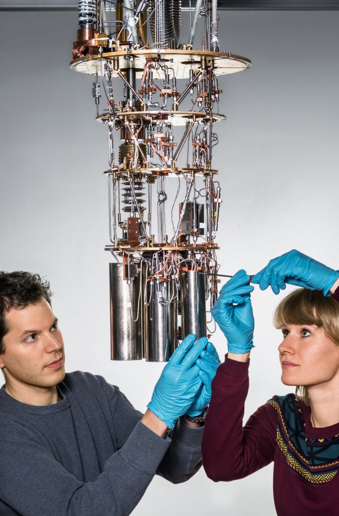
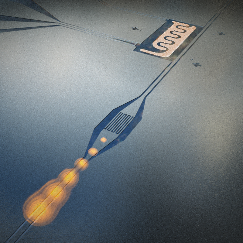
Achieving certifiably perfect randomness with quantum technology
(2026-05-28)
[...]
Nathan Lacroix wins Division of Quantum Information Thesis Award of the American Physical Society
(2026-03-19)
[...]
Functional building blocks for lattice-surgery on superconducting qubits
(2026-02-02)
[...]
New publication in Physical Review Research
(2026-01-16)
[...]